
2.6: Electron Microscopy
- Page ID
- 160509

\( \newcommand{\vecs}[1]{\overset { \scriptstyle \rightharpoonup} {\mathbf{#1}} } \)
\( \newcommand{\vecd}[1]{\overset{-\!-\!\rightharpoonup}{\vphantom{a}\smash {#1}}} \)
\( \newcommand{\dsum}{\displaystyle\sum\limits} \)
\( \newcommand{\dint}{\displaystyle\int\limits} \)
\( \newcommand{\dlim}{\displaystyle\lim\limits} \)
\( \newcommand{\id}{\mathrm{id}}\) \( \newcommand{\Span}{\mathrm{span}}\)
( \newcommand{\kernel}{\mathrm{null}\,}\) \( \newcommand{\range}{\mathrm{range}\,}\)
\( \newcommand{\RealPart}{\mathrm{Re}}\) \( \newcommand{\ImaginaryPart}{\mathrm{Im}}\)
\( \newcommand{\Argument}{\mathrm{Arg}}\) \( \newcommand{\norm}[1]{\| #1 \|}\)
\( \newcommand{\inner}[2]{\langle #1, #2 \rangle}\)
\( \newcommand{\Span}{\mathrm{span}}\)
\( \newcommand{\id}{\mathrm{id}}\)
\( \newcommand{\Span}{\mathrm{span}}\)
\( \newcommand{\kernel}{\mathrm{null}\,}\)
\( \newcommand{\range}{\mathrm{range}\,}\)
\( \newcommand{\RealPart}{\mathrm{Re}}\)
\( \newcommand{\ImaginaryPart}{\mathrm{Im}}\)
\( \newcommand{\Argument}{\mathrm{Arg}}\)
\( \newcommand{\norm}[1]{\| #1 \|}\)
\( \newcommand{\inner}[2]{\langle #1, #2 \rangle}\)
\( \newcommand{\Span}{\mathrm{span}}\) \( \newcommand{\AA}{\unicode[.8,0]{x212B}}\)
\( \newcommand{\vectorA}[1]{\vec{#1}} % arrow\)
\( \newcommand{\vectorAt}[1]{\vec{\text{#1}}} % arrow\)
\( \newcommand{\vectorB}[1]{\overset { \scriptstyle \rightharpoonup} {\mathbf{#1}} } \)
\( \newcommand{\vectorC}[1]{\textbf{#1}} \)
\( \newcommand{\vectorD}[1]{\overrightarrow{#1}} \)
\( \newcommand{\vectorDt}[1]{\overrightarrow{\text{#1}}} \)
\( \newcommand{\vectE}[1]{\overset{-\!-\!\rightharpoonup}{\vphantom{a}\smash{\mathbf {#1}}}} \)
\( \newcommand{\vecs}[1]{\overset { \scriptstyle \rightharpoonup} {\mathbf{#1}} } \)
\(\newcommand{\longvect}{\overrightarrow}\)
\( \newcommand{\vecd}[1]{\overset{-\!-\!\rightharpoonup}{\vphantom{a}\smash {#1}}} \)
\(\newcommand{\avec}{\mathbf a}\) \(\newcommand{\bvec}{\mathbf b}\) \(\newcommand{\cvec}{\mathbf c}\) \(\newcommand{\dvec}{\mathbf d}\) \(\newcommand{\dtil}{\widetilde{\mathbf d}}\) \(\newcommand{\evec}{\mathbf e}\) \(\newcommand{\fvec}{\mathbf f}\) \(\newcommand{\nvec}{\mathbf n}\) \(\newcommand{\pvec}{\mathbf p}\) \(\newcommand{\qvec}{\mathbf q}\) \(\newcommand{\svec}{\mathbf s}\) \(\newcommand{\tvec}{\mathbf t}\) \(\newcommand{\uvec}{\mathbf u}\) \(\newcommand{\vvec}{\mathbf v}\) \(\newcommand{\wvec}{\mathbf w}\) \(\newcommand{\xvec}{\mathbf x}\) \(\newcommand{\yvec}{\mathbf y}\) \(\newcommand{\zvec}{\mathbf z}\) \(\newcommand{\rvec}{\mathbf r}\) \(\newcommand{\mvec}{\mathbf m}\) \(\newcommand{\zerovec}{\mathbf 0}\) \(\newcommand{\onevec}{\mathbf 1}\) \(\newcommand{\real}{\mathbb R}\) \(\newcommand{\twovec}[2]{\left[\begin{array}{r}#1 \\ #2 \end{array}\right]}\) \(\newcommand{\ctwovec}[2]{\left[\begin{array}{c}#1 \\ #2 \end{array}\right]}\) \(\newcommand{\threevec}[3]{\left[\begin{array}{r}#1 \\ #2 \\ #3 \end{array}\right]}\) \(\newcommand{\cthreevec}[3]{\left[\begin{array}{c}#1 \\ #2 \\ #3 \end{array}\right]}\) \(\newcommand{\fourvec}[4]{\left[\begin{array}{r}#1 \\ #2 \\ #3 \\ #4 \end{array}\right]}\) \(\newcommand{\cfourvec}[4]{\left[\begin{array}{c}#1 \\ #2 \\ #3 \\ #4 \end{array}\right]}\) \(\newcommand{\fivevec}[5]{\left[\begin{array}{r}#1 \\ #2 \\ #3 \\ #4 \\ #5 \\ \end{array}\right]}\) \(\newcommand{\cfivevec}[5]{\left[\begin{array}{c}#1 \\ #2 \\ #3 \\ #4 \\ #5 \\ \end{array}\right]}\) \(\newcommand{\mattwo}[4]{\left[\begin{array}{rr}#1 \amp #2 \\ #3 \amp #4 \\ \end{array}\right]}\) \(\newcommand{\laspan}[1]{\text{Span}\{#1\}}\) \(\newcommand{\bcal}{\cal B}\) \(\newcommand{\ccal}{\cal C}\) \(\newcommand{\scal}{\cal S}\) \(\newcommand{\wcal}{\cal W}\) \(\newcommand{\ecal}{\cal E}\) \(\newcommand{\coords}[2]{\left\{#1\right\}_{#2}}\) \(\newcommand{\gray}[1]{\color{gray}{#1}}\) \(\newcommand{\lgray}[1]{\color{lightgray}{#1}}\) \(\newcommand{\rank}{\operatorname{rank}}\) \(\newcommand{\row}{\text{Row}}\) \(\newcommand{\col}{\text{Col}}\) \(\renewcommand{\row}{\text{Row}}\) \(\newcommand{\nul}{\text{Nul}}\) \(\newcommand{\var}{\text{Var}}\) \(\newcommand{\corr}{\text{corr}}\) \(\newcommand{\len}[1]{\left|#1\right|}\) \(\newcommand{\bbar}{\overline{\bvec}}\) \(\newcommand{\bhat}{\widehat{\bvec}}\) \(\newcommand{\bperp}{\bvec^\perp}\) \(\newcommand{\xhat}{\widehat{\xvec}}\) \(\newcommand{\vhat}{\widehat{\vvec}}\) \(\newcommand{\uhat}{\widehat{\uvec}}\) \(\newcommand{\what}{\widehat{\wvec}}\) \(\newcommand{\Sighat}{\widehat{\Sigma}}\) \(\newcommand{\lt}{<}\) \(\newcommand{\gt}{>}\) \(\newcommand{\amp}{&}\) \(\definecolor{fillinmathshade}{gray}{0.9}\)- Identify the advantages and limitations of EM compared to light microscopy
- Distinguish between TEM and SEM in terms of image production, resolution and types of samples analyzed
Electron Microscopy
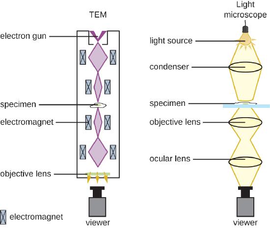
The maximum theoretical resolution of images created by light microscopes is ultimately limited by the wavelengths of visible light. Most light microscopes can only magnify 1000⨯, and a few can magnify up to 1500⨯, but this does not begin to approach the magnifying power of an electron microscope (EM), which uses short-wavelength electron beams rather than light to increase magnification and resolution.
Electrons, like electromagnetic radiation, can behave as waves, but with wavelengths of 0.005 nm, they can produce much better resolution than visible light. An EM can produce a sharp image that is magnified up to 100,000⨯. Thus, EMs can resolve subcellular structures as well as some molecular structures (e.g., single strands of DNA); however, electron microscopy cannot be used on living material because of the methods needed to prepare the specimens.
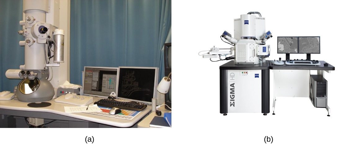
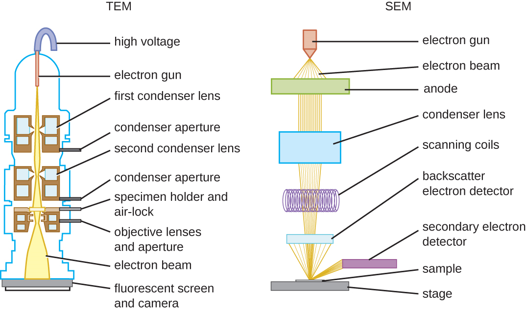
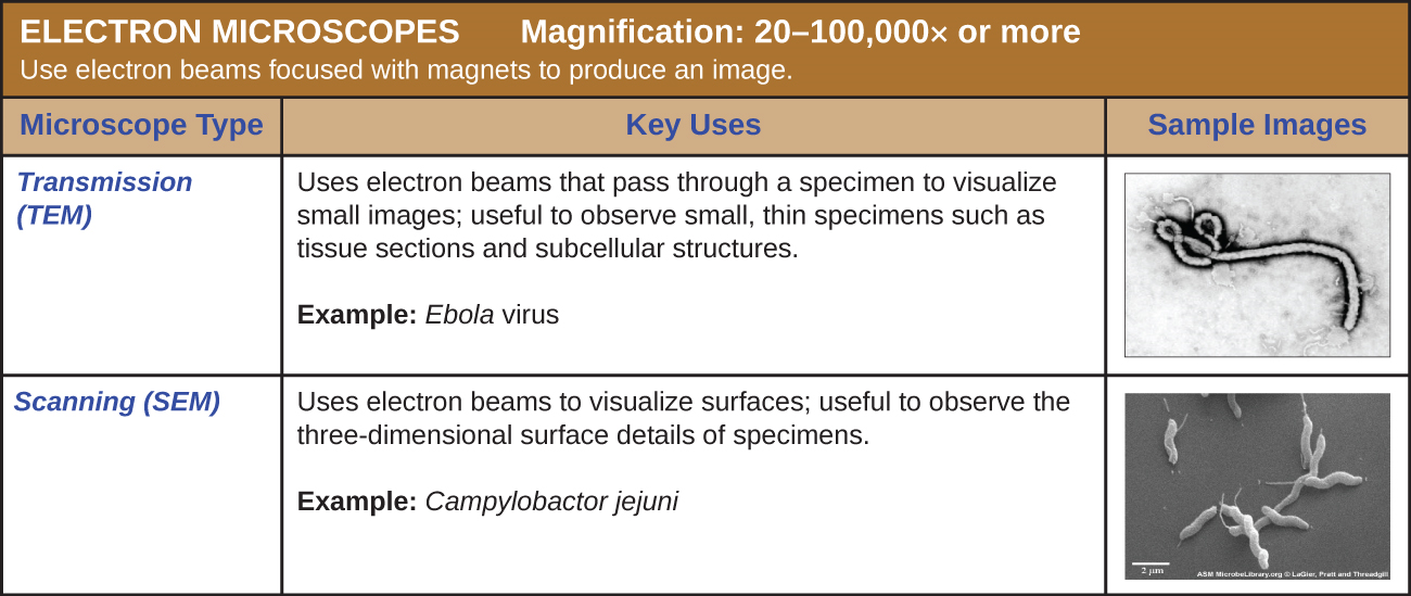
There are two basic types of EM: the transmission electron microscope (TEM) and the scanning electron microscope (SEM)(Figure \(\PageIndex{10}\)). The TEM is somewhat analogous to the brightfield light microscope in terms of the way it functions. However, it uses an electron beam from above the specimen that is focused using a magnetic lens (rather than a glass lens) and projected through the specimen onto a detector. Electrons pass through the specimen, and then the detector captures the image (Figure \(\PageIndex{11}\)).
For electrons to pass through the specimen in a TEM, the specimen must be extremely thin (20–100 nm thick). The image is produced because of varying opacity in various parts of the specimen. This opacity can be enhanced by staining the specimen with materials such as heavy metals, which are electron dense. TEM requires that the beam and specimen be in a vacuum and that the specimen be very thin and dehydrated. The specific steps needed to prepare a specimen for observation under an EM are discussed in detail in the next section.
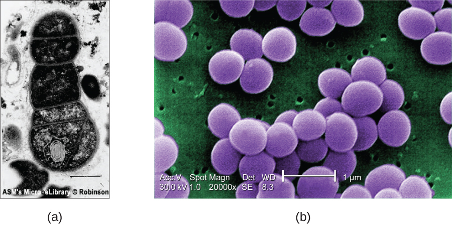
SEMs form images of surfaces of specimens, usually from electrons that are knocked off of specimens by a beam of electrons. This can create highly detailed images with a three-dimensional appearance that are displayed on a monitor (Figure \(\PageIndex{12}\)). Typically, specimens are dried and prepared with fixatives that reduce artifacts, such as shriveling, that can be produced by drying, before being sputter-coated with a thin layer of metal such as gold. Whereas transmission electron microscopy requires very thin sections and allows one to see internal structures such as organelles and the interior of membranes, scanning electron microscopy can be used to view the surfaces of larger objects (such as a pollen grain) as well as the surfaces of very small samples (Figure \(\PageIndex{13}\)). Some EMs can magnify an image up to 2,000,000⨯.1
Query \(\PageIndex{1}\)
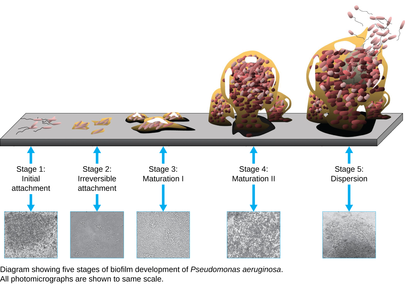
A biofilm is a complex community of one or more microorganism species, typically forming as a slimy coating attached to a surface because of the production of an extrapolymeric substance (EPS) that attaches to a surface or at the interface between surfaces (e.g., between air and water). In nature, biofilms are abundant and frequently occupy complex niches within ecosystems (Figure \(\PageIndex{14}\)). In medicine,biofilms can coat medical devices and exist within the body. Because they possess unique characteristics, such as increased resistance against the immune system and to antimicrobial drugs, biofilms are of particular interest to microbiologists and clinicians alike.
Because biofilms are thick, they cannot be observed very well using light microscopy; slicing a biofilm to create a thinner specimen might kill or disturb the microbial community. Confocal microscopy provides clearer images of biofilms because it can focus on one z-plane at a time and produce a three-dimensional image of a thick specimen. Fluorescent dyes can be helpful in identifying cells within the matrix. Additionally, techniques such as immunofluorescence and fluorescence in situ hybridization (FISH), in which fluorescent probes are used to bind to DNA, can be used.
Electron microscopy can be used to observe biofilms, but only after dehydrating the specimen, which produces undesirable artifacts and distorts the specimen. In addition to these approaches, it is possible to follow water currents through the shapes (such as cones and mushrooms) of biofilms, using video of the movement of fluorescently coated beads (Figure \(\PageIndex{15}\)).
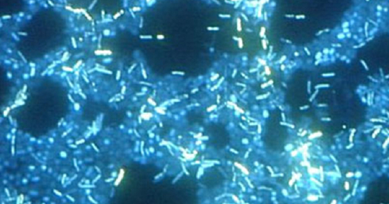
Scanning Probe Microscopy
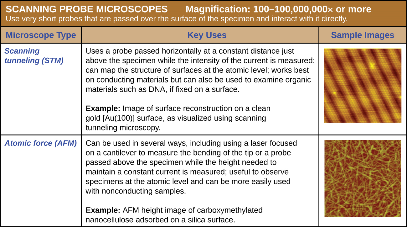
A scanning probe microscope does not use light or electrons, but rather very sharp probes that are passed over the surface of the specimen and interact with it directly. This produces information that can be assembled into images with magnifications up to 100,000,000⨯. Such large magnifications can be used to observe individual atoms on surfaces. To date, these techniques have been used primarily for research rather than for diagnostics.
There are two types of scanning probe microscope: the scanning tunneling microscope (STM) and the atomic force microscope (AFM). An STM uses a probe that is passed just above the specimen as a constant voltage bias creates the potential for an electric current between the probe and the specimen. This current occurs via quantum tunneling of electrons between the probe and the specimen, and the intensity of the current is dependent upon the distance between the probe and the specimen. The probe is moved horizontally above the surface and the intensity of the current is measured. Scanning tunneling microscopy can effectively map the structure of surfaces at a resolution at which individual atoms can be detected.
Similar to an STM, AFMs have a thin probe that is passed just above the specimen. However, rather than measuring variations in the current at a constant height above the specimen, an AFM establishes a constant current and measures variations in the height of the probe tip as it passes over the specimen. As the probe tip is passed over the specimen, forces between the atoms (van der Waals forces, capillary forces, chemical bonding, electrostatic forces, and others) cause it to move up and down. Deflection of the probe tip is determined and measured using Hooke’s law of elasticity, and this information is used to construct images of the surface of the specimen with resolution at the atomic level (Figure \(\PageIndex{16}\)).
Query \(\PageIndex{1}\)
Key Concepts and Summary
- Electron microscopy focuses electrons on the specimen using magnets, producing much greater magnification than light microscopy. The transmission electron microscope (TEM) and scanning electron microscope (SEM) are two common forms.
- Scanning probe microscopy produces images of even greater magnification by measuring feedback from sharp probes that interact with the specimen. Probe microscopes include the scanning tunneling microscope (STM) and the atomic force microscope (AFM).
Footnotes
- 1 “JEM-ARM200F Transmission Electron Microscope,” JEOL USA Inc, www.jeolusa.com/PRODUCTS/Tran...specifications. Accessed 8/28/2015.